
LMH6554LE-EVAL
用于 LMH6554 的评估板
AN-1945 LMH6554LE-EVAL High Speed Differential
Amplifier Evaluation Board
General Description
The LMH6554LE−EVAL evaluation board is designed to aid in the characterization of Texas Instruments LMH6554 fully differential amplifier in an 14 lead UQFN package. The LMH6554 is part of the LMH™ high-speed amplifier family.
Use the evaluation board as a guide for high frequency layout and as a tool to aid in device testing and characterization.
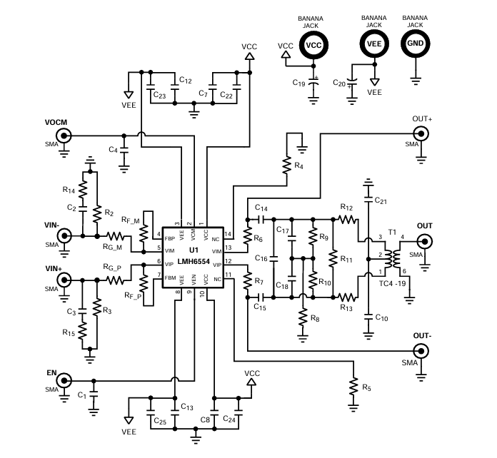
The evaluation board schematic is shown in Figure 1. For recommended for component values, see the device-specific data sheets.
2. Basic Operation
The LMH6554LE−EVAL evaluation board has been set up to provide maximum flexibility for evaluating TI’s differential LMH6554 operational amplifier. The board supports fully differential operation as well as single-ended to differential and single-ended to single-ended operation. For fully differential operation, use resistors R2 and R3 to set the input impedance of the amplifier. The differential input resistance will be equal to 2*R2 || 2*RG_M . Where R2 = R3 and RG_M = RG_P . In this mode resistors RG_M , RG_F , RF_M and RF_P set the gain of the amplifier. Amplifier gain = RF_M /RG_M = RF_P /RG_P where RG_M = RG_P and RF_M = RF_P . For more details on gain component value selections, see Table 2. For single-ended input mode of operation, the input and termination resistance must be properly configured to give the correct gain and input impedance (RIN ). For example, in the case of the LMH6554, if a gain of 2 V/V is desired, R2 = R3 = 76.8 Ω, RG_M = RG_P = 90 Ω, RF_M = RF_P = 200 Ω, C2 and R14 = OPEN, C3 = 0.1 µF, and R15 = 50 Ω, which will make RIN = 50 Ω at the most positive node of R3 looking into RG_M . Further details of single-ended input mode calculations can be found in the LMH6554 2.8 GHz Ultra Linear Fully Differential Amplifier Data Sheet (SNOSB30). Components C3 = 0.1 µF and R15 = 50 Ω should be used to AC-couple and balance the inputs, otherwise can be left empty. In this example the input signal would be connected to the VIN- input. For more details on gain component value selections, see Table 1.
For differential output applications, load R6 and R7 with the desired values to match the output load and leave C14 and C15 empty. Typically to match a test equipment, R6 = R7 = 50 Ω.
If single-ended output is desired an output transformer such as the TC4-19 from mini circuits can be utilized. The TC4-19 has a 4:1 impedance ratio (2:1 turns/voltage ratio). This is particularly useful for interfacing to a 50 Ω test equipment. When referencing the transformer data sheet, the LMH6554LE−EVAL evaluation board has the primary windings on the output side of the evaluation board and the amplifier is driving the secondary windings. This provides a step down transformation from the differential amplifier output to the test equipment. The center-tapped secondary winding also allows a differential to single ended conversion (Balun). The impedance seen by the differential amplifier = (R6 + R7 + RL *4), where RL is the impedance from pin 4 of the transformer to the load. For example, if RL = 50 Ω for the test equipment, to achieve an impedance of 500 Ω seen by the LMH6554 differential output R6 = R7 = 150 Ω with C14 = C15 = R12 = R13 = 0 Ω. The LMH6554LE−EVAL board is equipped with pads to add additional filtering schemes using C14- C18 and R8- R13 .
Pin 9 on the LMH6554 device is the enable (VEN) pin that can be used to disable the device with an external signal. Pin 11 and 14 have no internal package connections and should be connected to analog ground by using 0 Ω resistors for R4 and R5 . For more details, see the LMH6554 2.8 GHz Ultra Linear Fully Differential Amplifier Data Sheet (SNOSB30)
3. Layout Considerations
The printed circuit board (PCB) layout and supply bypassing play major roles in determining high frequency performance. Use these evaluation boards as a guide when designing your own board and follow these steps to optimize high frequency performance:
1. Symmetry is of the utmost importance.
2. Use precision resistors 0.1% or 0.01%.
3. Use a ground plane.
4. Include large ( ~ 10 μF) ceramic capacitors on both supplies (C19 and C20).
5. Near the device use ceramic capacitors 0.1 μF for C22–25 and 0.01 μF for C7, C8, C12, and C13 from supplies to ground.
6. Remove the ground and power planes from under and around the part, especially the input and outputpins.
7. Minimize all trace lengths.
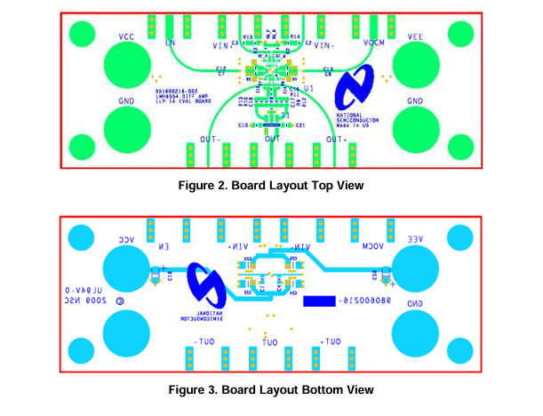
8. Use terminated and matched transmission lines for long traces.Sample artwork for the LMH6554LE−EVAL evaluation board is shown in Figure 2 and Figure 3.
4. Measurement Hints
Balance, CMRR and HD2 are highly dependent on resistor matching. Use 0.1 or 0.01% resistors.
The LMH6554LE−EVAL™ evaluation board is designed for differential or single-ended output measurements, but not both at the same time. When not using the transformer make sure to leave C14 and C15 empty. Likewise, when making single-ended output measurements populate components C14 , C15 , R12 and R13 .
Many differential amplifiers are optimized for the higher impedances represented by most ADCs.
On a differential amplifier both inputs are inverting, keep parasitic capacitance to a minimum on both inputs. Also, using probes of any kind on a differential circuit is not recommended.
5. LMH6554LE_EVALSchematic
6. LMH6554LE_EVAL Board Layout Views
- 苏州杭晶电子入驻工之芯商城,成为优质供应商
- TPS7A30-49EVM-567_TI(德州仪器)中文资料_英文资料_价格_PDF手册
- TLA2024EVM-PDK_TI(德州仪器)中文资料_英文资料_价格_PDF手册
- INA229_239EVM_TI(德州仪器)中文资料_英文资料_价格_PDF手册
- DAC8832EVM-PDK _TI(德州仪器)中文资料_英文资料_价格_PDF手册
- LP8557IEVM_TI(德州仪器)中文资料_英文资料_价格_PDF手册
- LAUNCHXL-F28027F TI(德州仪器)中文资料_英文资料_价格_PDF手册
- DLPDLCR160CPEVM DLP160CP TI(德州仪器)中文资料_英文资料_价格_PDF手册
- THS4631DDAEVM TI(德州仪器)中文资料_英文资料_价格_PDF手册
- DAC3482EVM TI(德州仪器)中文资料_英文资料_价格_PDF手册
- THS4302EVM TI(德州仪器)中文资料_英文资料_价格_PDF手册
- ADS7038Q1EVM-PDK_TI(德州仪器)中文资料_英文资料_价格_PDF手册
- LM3450AEV230V30/NOPB_TI(德州仪器)中文资料_英文资料_价格_PDF手册
- TPS72728DSEEVM-406_TI(德州仪器)中文资料_英文资料_价格_PDF手册
- WL1835MODCOM8A_TI(德州仪器)中文资料_英文资料_价格_PDF手册
 工商网监