ATL431LIEVM
1 Overview
The ATL431LIEVM is an adjustable voltage reference evaluation module that demonstrates the ATL431LI integrated circuit in its new X2SON (DQN) small form factor from Texas Instruments (TI). The ATL431LI is a low-power counterpart to the TL431LI, having lower minimum cathode current (Ikmin = 80 μA vs 1.0 mA). Like TL431LI, ATL431LI is used in conjunction with its key components to behave as a single voltage reference, error amplifier, voltage clamp or comparator with integrated reference. The ATL431LI can be operated and adjusted to cathode voltages from 2.5 V to 36 V, making this part optimum for a wide range of end equipment in industrial, auto, telecom, and computing. In order for this device to behave as a shunt regulator or error amplifier, > 80 μA (Imin(max)) must be supplied into the cathode pin. Under this condition, feedback can be applied from the Cathode and Ref pins to create a replica of the internal reference voltage.
The ATL431LIEVM is configured with a fix voltage output and load capacitor. A test point can be connected to an external power supply to provide power. All of the ATL431 input and output pins are accessible for external connection via test points. For users looking for a EVM to test the SOT23-3 variant, use the ATL431 EVM because it is compatible with the ATL431LI.
1.1 ATL431LIEVM Features
• X2SON land pattern for the ATL431LI in X2SON
• Footprints for resistors
• Multiple test points outputs for voltage measurement
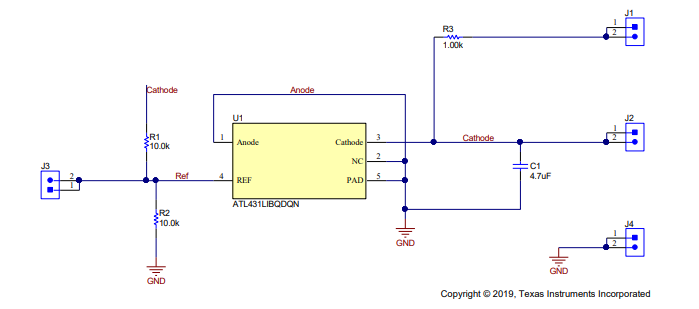
1.2 Schematic
The schematic for the ATL431LIEVM is illustrated in Figure 1.

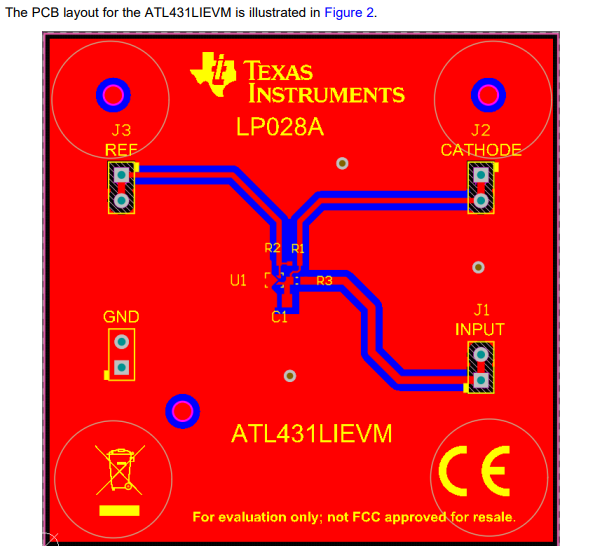
1.3 PCB
The PCB layout for the ATL431LIEVM is illustrated in Figure 2

2 Quick Setup Guide
This section describes the setup to quickly check the functionality of the ATL431LIEVM.
2.1 Electrostatic Discharge Warning
Many of the components on the ATL431LIEVM are susceptible to damage by electrostatic discharge (ESD). Customers are advised to observe proper ESD handling precautions when unpacking and handling the EVM, including the use of a grounded wrist strap at an approved ESD workstation.
2.2 Unpacking the EVM
After opening the ATL431LIEVM package, ensure that the following is included: 1 pc. ATL431LIEVM board using one ATL431LIBQDQN
2.3 Power Supply Setup and Functional Test
A 10-V power supply capable of 10 mA of current is required.
Connect the positive power supply lead to the “INPUT” on J1. Connect the negative power supply lead to "GND" on J4.
Connect a voltmeter positive terminal to "CATHODE" on J2. Connect the negative voltmeter terminal to "GND" on J4.
3 EVM Theory and Operation
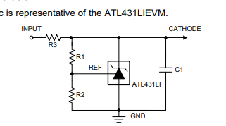
The following schematic is representative of the ATL431LIEVM.

The ATL431LIEVM is designed to allow users to evaluate the configuration in Figure 3. With the provided footprints, a user can change the passive components to better suit their application. As shown in Figure 2, the EVM is designed to allow users to evaluate the small form factor of the ATL431LI in X2SON (DQN). This EVM also has the land pattern for the ATL431LI X2SON which allows users to test the device in their system with the provided pins.
4 Test Modes
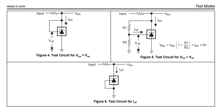
The ATL431LIEVM can be configured to measure practically every parameter shown in the typical characteristics of the datasheet. This configuration might require the switching of the passive components, such as R1 and R2 , to other values.

- LM3450AEV230V30/NOPB_TI(德州仪器)中文资料_英文资料_价格_PDF手册
- TPS72728DSEEVM-406_TI(德州仪器)中文资料_英文资料_价格_PDF手册
- WL1835MODCOM8A_TI(德州仪器)中文资料_英文资料_价格_PDF手册
- TAS5424BQ1DKDEVM_TI(德州仪器)中文资料_英文资料_价格_PDF手册
- ADS7042EVM-PDK_TI(德州仪器)中文资料_英文资料_价格_PDF手册
- TMDS570LS31HDK_TI(德州仪器)中文资料_英文资料_价格_PDF手册
- VCA8500BOARD_TI(德州仪器)中文资料_英文资料_价格_PDF手册
- DEM-SOT223LDO_TI(德州仪器)中文资料_英文资料_价格_PDF手册
- DAC8564EVM_TI(德州仪器)中文资料_英文资料_价格_PDF手册
- ADS8412EVM _TI(德州仪器)中文资料_英文资料_价格_PDF手册
- TPS61500EVM-369_TI(德州仪器)中文资料_英文资料_价格_PDF手册
- TPS7A6050EVM_TI(德州仪器)中文资料_英文资料_价格_PDF手册
- ADC3244EVM_TI(德州仪器)中文资料_英文资料_价格_PDF手册
- TMS320F280025C_TI(德州仪器)中文资料_英文资料_价格_PDF手册
- THS3217EVM _TI(德州仪器)中文资料_英文资料_价格_PDF手册
