
 ADS5413EVM
1.1 Purpose
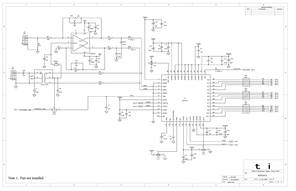
The ADS5413 EVM provides a platform for evaluating the ADS5413
analog-to-digital converter (ADC) under various signal, reference, and supply
conditions. This document should be used in combination with the EVM
schematic diagram supplied
1.2 EVM Basic Functions
Analog input to the ADC is provided via two external SMA connectors. The single-ended input the user provides is converted into a differential signal at the input of the device. One input uses a differential amplifier, while the other input is transformer coupled.
The EVM provides external SMA connectors for input of the ADC clock. The EVM allows the user to send a single-ended or differential clock to the ADC. Another SMA connector allows the user to send a second clock source to the output connector along with the digital data. This allows the user to provide the required setup and hold times of the output data with respect to the output clock. See the Clock Inputs section for proper configuration and operation.
Digital outputs from the EVM are via a 40-pin connector. The digital lines from the ADC are buffered before going to this connector. More information on these connectors can be found in the ADC output section.
Power connections to the EVM are via banana jack sockets. Separate sockets are provided for the ADC core, output drivers, and external reference/differential amplifier supplies
1.3 Power Requirements
The EVM can be powered directly with only a 3.3-V supply if using the ADC with 3.3-VDC output levels.
±5 V is required if using the differential amplifier input. 1.8 V is required for DRVDD if 1.8-V logic output levels are desired.
1.3.1 Voltage Limits
Exceeding the maximum input voltages can damage EVM components. Under voltage may cause improper operation of some or all of the EVM components.
2.1 PCB Layout
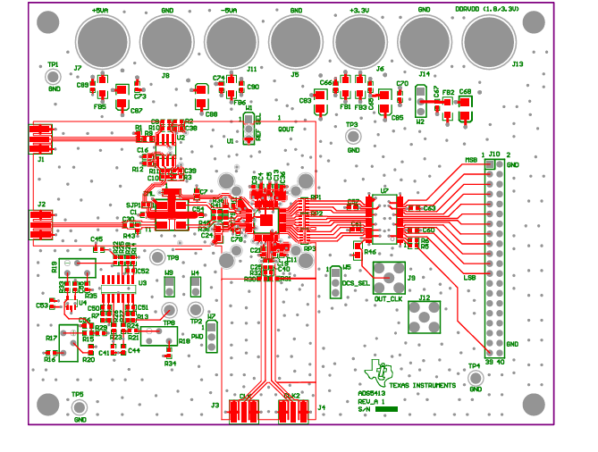
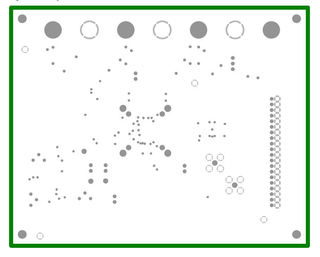
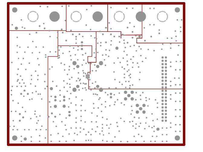
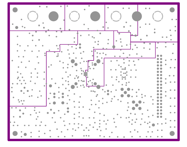
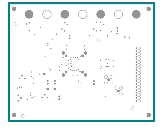
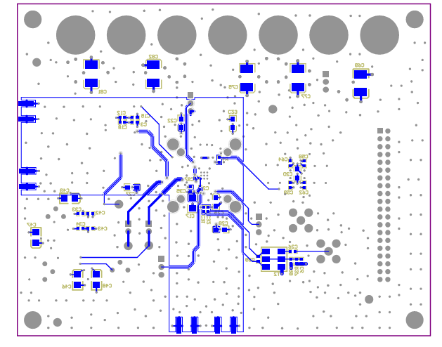
The EVM is constructed on a 6-layer, 4.25-inch × 5.3-inch, 0.062-inch thick PCB using FR−4 material. The individual layers are shown in Figure 2−1 through Figure 2−6.
- 苏州杭晶电子入驻工之芯商城,成为优质供应商
- TPS7A30-49EVM-567_TI(德州仪器)中文资料_英文资料_价格_PDF手册
- TLA2024EVM-PDK_TI(德州仪器)中文资料_英文资料_价格_PDF手册
- INA229_239EVM_TI(德州仪器)中文资料_英文资料_价格_PDF手册
- DAC8832EVM-PDK _TI(德州仪器)中文资料_英文资料_价格_PDF手册
- LP8557IEVM_TI(德州仪器)中文资料_英文资料_价格_PDF手册
- LAUNCHXL-F28027F TI(德州仪器)中文资料_英文资料_价格_PDF手册
- DLPDLCR160CPEVM DLP160CP TI(德州仪器)中文资料_英文资料_价格_PDF手册
- THS4631DDAEVM TI(德州仪器)中文资料_英文资料_价格_PDF手册
- DAC3482EVM TI(德州仪器)中文资料_英文资料_价格_PDF手册
- THS4302EVM TI(德州仪器)中文资料_英文资料_价格_PDF手册
- ADS7038Q1EVM-PDK_TI(德州仪器)中文资料_英文资料_价格_PDF手册
- LM3450AEV230V30/NOPB_TI(德州仪器)中文资料_英文资料_价格_PDF手册
- TPS72728DSEEVM-406_TI(德州仪器)中文资料_英文资料_价格_PDF手册
- WL1835MODCOM8A_TI(德州仪器)中文资料_英文资料_价格_PDF手册
 工商网监
工商网监