
OPAMPEVM-SOT23
采用 MSOP/SOIC/SOT-23 封装的没有关断功能的单/双路运算放大器通用 EVM
1.Overview
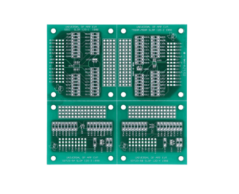
The OPAMPEVM-SOT23 is a general purpose blank circuit board that simplifies evaluation of surface-mount op amps. The evaluation module board design allows many different circuits to be constructed easily and quickly. The board has four separate circuit development areas that can be snapped apart and separated. Two of the areas are specifically designed for SOT23-5 package OPAMP's; the other two areas support SOIC-8 and MSOP-8 type packages. See the OPAMPEVM-SOT23 Users Guide for additional information. Note: These boards are unpopulated, so remember to order your op amp device samples.
1.1 Design Features
The evaluation module board design allows many different circuits to be constructed easily and quickly. The board has four separate circuit development areas that can be snapped apart and separated. Areas 100 and 200 are for dual op amps in the SOIC and TSSOP/MSOP packages. Areas 300 and 400 are for SOT23–5 single operational amplifier packages. A few possible circuits are listed below:
Voltage Follower
Noninverting Amplifier
Inverting Amplifier
Simple or Algebraic Summing Amplifier
Difference Amplifier
Current-to-Voltage Converter
Voltage–to-Current Converter
Integrator/Low-Pass Filter
Differentiator/High-Pass Filter
Instrumentation Amplifier
Sallen-Key Filter
The EVM PCB is of two-layer construction, with a ground plane on the solder side. Circuit performance should be comparable to final production designs.
1.2 Power Requirements
The devices and designs that are used dictate the input power requirements. Three input terminals are provided for each area of the board:
Vx+ Positive input power for area x00 i.e., V1+ ⇒ area 100
GNDx Ground reference for area x00 i.e., GND2 ⇒ area 200
Vx Negative input power for area x00 i.e., V4– ⇒ area 400
Each area has four bypass capacitors, two for the positive supply, and two for the negative supply. Each supply should have a 1-mF to 10-mF capacitor for low frequency bypassing and a 0.01-mF to 0.1-mF capacitor for high frequency bypassing.
When using single supply circuits, the negative supply is shorted to ground by bridging Cx02 or Cx06, and power input is between Vx+ and GNDx. The voltage reference circuitry is provided for single supply applications that require a reference voltage to be generated.
This chapter describes and shows the universal op amp EVM board layout and the relationships between the four areas.
2.1 Physical Considerations
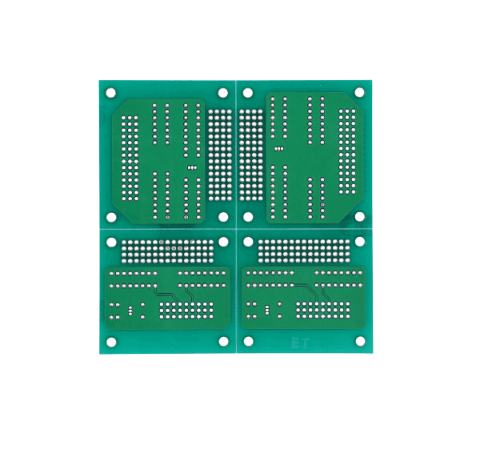
The EVM board has four circuit development areas. If a specific area is desired, it can be separated from the others by breaking along the score lines. The circuit layout in each area supports an op amp package, voltage reference, and ancillary devices. The op amp package is unique to each area as described in the following paragraphs. The voltage reference and supporting devices are the same for all areas. Surface-mount or through-hole devices can be used for all capacitors and resistors on the board.
The voltage reference can be either surface mount or through hole. If surface mount is desired, the TLV431ACDBV5 or TLV431AIDBV5 adjustable shunt regulators can be used. If through hole is desired, then the TLV431ACLP, TLV431AILP, TL431CLP, TL431ACLP, TL431ILP or TL431AILP adjustable shunt regulators can be used. Refer to Texas Instruments’ Power Supply Circuits Data Book (literature number SLVD002) for details on usage of these shunt regulators.
Each passive component, resistor and capacitor, has a surface-mount 1206 foot print with through holes at 0.2″ spacing on the outside of the 1206 pads. Therefore, either surface-mount or through-hole parts can be used.
- 苏州杭晶电子入驻工之芯商城,成为优质供应商
- TPS7A30-49EVM-567_TI(德州仪器)中文资料_英文资料_价格_PDF手册
- TLA2024EVM-PDK_TI(德州仪器)中文资料_英文资料_价格_PDF手册
- INA229_239EVM_TI(德州仪器)中文资料_英文资料_价格_PDF手册
- DAC8832EVM-PDK _TI(德州仪器)中文资料_英文资料_价格_PDF手册
- LP8557IEVM_TI(德州仪器)中文资料_英文资料_价格_PDF手册
- LAUNCHXL-F28027F TI(德州仪器)中文资料_英文资料_价格_PDF手册
- DLPDLCR160CPEVM DLP160CP TI(德州仪器)中文资料_英文资料_价格_PDF手册
- THS4631DDAEVM TI(德州仪器)中文资料_英文资料_价格_PDF手册
- DAC3482EVM TI(德州仪器)中文资料_英文资料_价格_PDF手册
- THS4302EVM TI(德州仪器)中文资料_英文资料_价格_PDF手册
- ADS7038Q1EVM-PDK_TI(德州仪器)中文资料_英文资料_价格_PDF手册
- LM3450AEV230V30/NOPB_TI(德州仪器)中文资料_英文资料_价格_PDF手册
- TPS72728DSEEVM-406_TI(德州仪器)中文资料_英文资料_价格_PDF手册
- WL1835MODCOM8A_TI(德州仪器)中文资料_英文资料_价格_PDF手册
 工商网监
工商网监