
LP5910DRV18EVM
1 Introduction
The Texas Instruments LP5910DRV evaluation module (EVM) helps designers evaluate the operation and performance of the LP5910 LDO voltage regulator. The LP5910DRV EVM contains one LP5910 LDO voltage regulator in the WSON / DRV package (see Table 1).

2 Setup
This section describes the jumpers and connectors on the EVM as well and how to properly connect, set up and use the LP5910DRV EVM.
The device has been designed to work with 1-µF input and output ceramic capacitors down to 0402 component size.
2.1 Input/Output Connector Descriptions
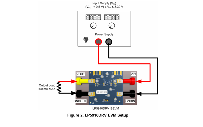
VIN and GNDIN are the connection terminals for the input supply. The VIN terminal is the positive connection, and the GNDIN terminal is the negative (that is, ground) connection.
VOUT and GNDOUT are the connection terminals for the output load. The VOUT terminal is the positive connection, and the GNDOUT terminal is the negative (that is, ground) connection.
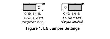
GND_EN_IN is a 3-pin terminal used to enable, or disable, the LP5910.
When the shunt is across EN_IN terminal pins the Enable (EN) pin is directly connected to VIN. The LP5910 will be enabled when VIN is applied.
When the shunt is across GND_EN terminal pins the EN pin is connected directly to GND. The LP5910 will be disabled
The shunt must be in place, or the EN terminal pin must be driven by an off-board supply, otherwise LP5910 EN pin is floating, and the EN status may be undefined. The default, and recommended, shunt position is across the EN_IN terminal pins (enabled).
2.2 Setup
The recommended operating input voltage range for the LP5910DRV EVM is : VOUT + 0.5 V (minimum) to 3.3 V (maximum).
A load should be applied between the VOUT terminal and the GNDOUT terminal for proper operation. Load current should be maintained between 1 mA and 300 mA.
- 苏州杭晶电子入驻工之芯商城,成为优质供应商
- TPS7A30-49EVM-567_TI(德州仪器)中文资料_英文资料_价格_PDF手册
- TLA2024EVM-PDK_TI(德州仪器)中文资料_英文资料_价格_PDF手册
- INA229_239EVM_TI(德州仪器)中文资料_英文资料_价格_PDF手册
- DAC8832EVM-PDK _TI(德州仪器)中文资料_英文资料_价格_PDF手册
- LP8557IEVM_TI(德州仪器)中文资料_英文资料_价格_PDF手册
- LAUNCHXL-F28027F TI(德州仪器)中文资料_英文资料_价格_PDF手册
- DLPDLCR160CPEVM DLP160CP TI(德州仪器)中文资料_英文资料_价格_PDF手册
- THS4631DDAEVM TI(德州仪器)中文资料_英文资料_价格_PDF手册
- DAC3482EVM TI(德州仪器)中文资料_英文资料_价格_PDF手册
- THS4302EVM TI(德州仪器)中文资料_英文资料_价格_PDF手册
- ADS7038Q1EVM-PDK_TI(德州仪器)中文资料_英文资料_价格_PDF手册
- LM3450AEV230V30/NOPB_TI(德州仪器)中文资料_英文资料_价格_PDF手册
- TPS72728DSEEVM-406_TI(德州仪器)中文资料_英文资料_价格_PDF手册
- WL1835MODCOM8A_TI(德州仪器)中文资料_英文资料_价格_PDF手册
 工商网监
工商网监