
BQ25792EVM
1 Introduction
The BQ25792 and BQ25798 (BQ25792/8) is an integrated switched-mode buck-boost battery charge management device in QFN package. It is intended to charge 1- to 4-series cell Li-ion and Li-polymer batteries. The charger features a narrow VDC architecture (NVDC) which allows the system to be regulated to a minimum value even if the battery is completely discharged. Additionally, the BQ25792/8 supports input source detection through D+ and D- which is compatible with USB2.0, USB3.0 power delivery, non-standard adapters, and high voltage adapters. With dual input source selection, USB OTG support, and an integrated 16-bit multi-channel analog-to-digital converter (ADC), the BQ25792/8 is a complete charging solution.
1.1 EVM Features
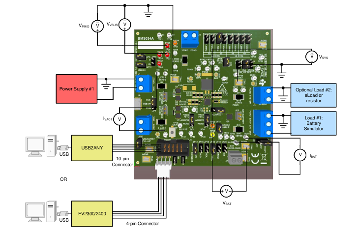
The BQ25792/8EVM is a complete module for evaluating the BQ25792/8 charger IC in the QFN package. Key features of this EVM include:
• Synchronous Switch Mode Buck-Boost Charger for 1s-4s Battery Configuration for 5-A Charging with 10-mA Resolution
• Support for 3.6-V to 24-V Wide Range of Input Sources USB Auto-Detect, USB PD and Wireless Input
• Dual Input Source Selector to Drive Bi-Directional Blocking NFETs
• Power up USB Port from Battery (USB OTG) with 2.8-V to 22-V OTG Output Voltage with 10-mV Resolution
• Low Battery Quiescent Current < 1 µA in Shutdown Mode
• BQ25798 has MPPT and backup mode features.
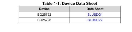
The device data sheet, listed in Table 1-1, provides detailed features and operation.
2 PCB Layout Guidelines
Careful placement of components is critical in order for the charger to meet specifications. The items below are listed in order of placement priority.
1. Place high frequency decoupling capacitors for PMID and SYS (C3 and C18 on the EVM) as close possible to their respective pins and ground pin on the same layer as the charger IC (in other words, no vias) in order to have the smallest current loop.
2. Place bulk capacitors for PMID and SYS as close possible to their respective pins and the charger's ground pin on the same layer as the charger IC on the same layer as the charger IC (in other words, no vias).
3. Place the REGN capacitor (C35) to ground and BTST capacitors (C6 and C8) to SW as close as possible to their respective pins only using vias for 1 side of each component if necessary.
4. Place high frequency decoupling capacitors for VBUS and BAT pins as close as possible to their respective pins. Use at least 2 vias per capacitor terminal if required.
5. Place bulk capacitors for VBUS and BAT pins as close as possible to their respective pins. Use at least 2 vias per capacitor terminal if required.
6. Place the inductor close to SW1 and SW2 pins. It is acceptable to use multiple vias to make these
connections as the vias are only adding small amounts of inductance and resistance to an inductor.
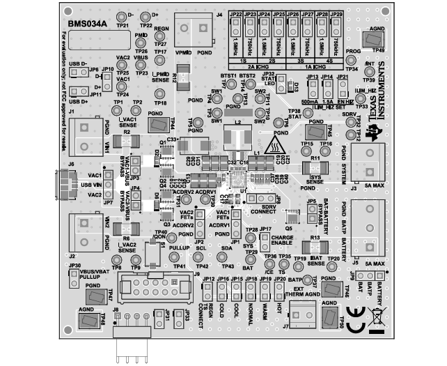
7. While this EVM has analog ground (AGND) and power ground (PGND) planes that connect close to the charge GND pin, two grounds not required. Resistors and capacitors used for setting sensitive nodes (for example, ILIM, TS) can use one common ground plane but with their ground terminals connected away from high current ground return paths containing switching noise.Note that this EM has test points and jumpers requiring traces out to the PCB edges. Routing these traces required some PCB layout compromises for less critical components than those listed in the first six items above.
3 Board Layout, Schematic and Bill of Materials
- 苏州杭晶电子入驻工之芯商城,成为优质供应商
- TPS7A30-49EVM-567_TI(德州仪器)中文资料_英文资料_价格_PDF手册
- TLA2024EVM-PDK_TI(德州仪器)中文资料_英文资料_价格_PDF手册
- INA229_239EVM_TI(德州仪器)中文资料_英文资料_价格_PDF手册
- DAC8832EVM-PDK _TI(德州仪器)中文资料_英文资料_价格_PDF手册
- LP8557IEVM_TI(德州仪器)中文资料_英文资料_价格_PDF手册
- LAUNCHXL-F28027F TI(德州仪器)中文资料_英文资料_价格_PDF手册
- DLPDLCR160CPEVM DLP160CP TI(德州仪器)中文资料_英文资料_价格_PDF手册
- THS4631DDAEVM TI(德州仪器)中文资料_英文资料_价格_PDF手册
- DAC3482EVM TI(德州仪器)中文资料_英文资料_价格_PDF手册
- THS4302EVM TI(德州仪器)中文资料_英文资料_价格_PDF手册
- ADS7038Q1EVM-PDK_TI(德州仪器)中文资料_英文资料_价格_PDF手册
- LM3450AEV230V30/NOPB_TI(德州仪器)中文资料_英文资料_价格_PDF手册
- TPS72728DSEEVM-406_TI(德州仪器)中文资料_英文资料_价格_PDF手册
- WL1835MODCOM8A_TI(德州仪器)中文资料_英文资料_价格_PDF手册
 工商网监